
Semiconductor equipement
Inspection and surface topology measurement of high accuracy molded parts for the semiconductor industry

Problem
Our customer, a semiconductor startup, needed to measure the surface topology of small molded parts at extremely high throughput. After testing dozens of off-the-shelf solutions, even the best was at least ten times too slow. They turned to us to develop a customized, high-speed topology inspection platform.

Solution
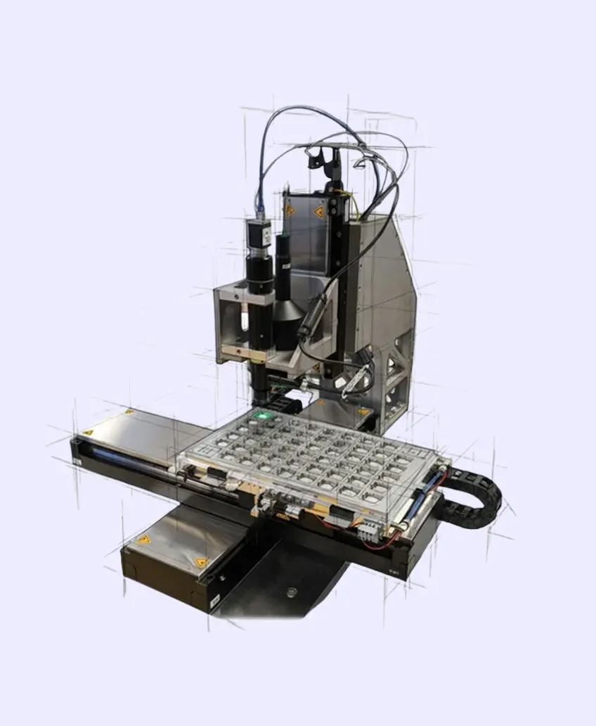
The customer goal was to prototype fast, we therefore created a fully customized system based on our standard platform, integrating a confocal sensor and vision camera with a high-speed motion stage and acquisition system. The analysis software was developed entirely in-house to reduce cost while maintaining maximum speed.

Result
The prototype was delivered in just seven months. Measurement accuracy was better than +/-1µm, while productivity skyrocketed from ~100 units per hour with off-the-shelf solutions to 1,000 units per hour using our customized metrology platform.